- 您现在的位置:买卖IC网 > Sheet目录337 > LH28F008SCHT-TE (Sharp Microelectronics)IC FLASH 8MBIT 85NS 40TSOP
�� �
�
�LHF08CTE�
�9�
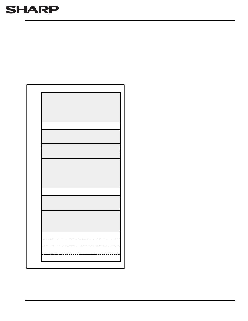
�3.5� Read� Identifier� Codes� Operation�
�The� read� identifier� codes� operation� outputs� the�
�manufacturer� code,� device� code,� block� lock�
�configuration� codes� for� each� block,� and� the� master�
�lock� configuration� code� (see� Figure� 4).� Using� the�
�manufacturer� and� device� codes,� the� system� CPU� can�
�automatically� match� the� device� with� its� proper�
�algorithms.� The� block� lock� and� master� lock�
�configuration� codes� identify� locked� and� unlocked�
�blocks� and� master� lock-bit� setting.�
�FFFFF�
�Reserved� for�
�3.6� Write�
�Writing� commands� to� the� CUI� enable� reading� of�
�device� data� and� identifier� codes.� They� also� control�
�inspection� and� clearing� of� the� status� register.� When�
�V� PP� =V� PPH1/2/3� ,� the� CUI� additionally� controls� block�
�erasure,� byte� write,� and� lock-bit� configuration.�
�The� Block� Erase� command� requires� appropriate�
�command� data� and� an� address� within� the� block� to� be�
�erased.� The� Byte� Write� command� requires� the�
�command� and� address� of� the� location� to� be� written.�
�Set� Master� and� Block� Lock-Bit� commands� require� the�
�command� and� address� within� the� device� (Master�
�Lock)� or� block� within� the� device� (Block� Lock)� to� be�
�locked.� The� Clear� Block� Lock-Bits� command� requires�
�the� command� and� address� within� the� device.�
�F0004�
�F0003�
�Future� Implementation�
�The� CUI� does� not� occupy� an� addressable� memory�
�location.� It� is� written� when� WE#� and� CE#� are� active.�
�F0002�
�F0001�
�Block� 15� Lock� Configuration� Code�
�Reserved� for�
�The� address� and� data� needed� to� execute� a� command�
�are� latched� on� the� rising� edge� of� WE#� or� CE#�
�(whichever� goes� high� first).� Standard� microprocessor�
�F0000�
�Future� Implementation�
�Block� 15�
�write� timings� are� used.� Figures� 16� and� 17� illustrate�
�WE#� and� CE#-controlled� write� operations.�
�1FFFF�
�(Blocks� 2� through� 14)�
�4� COMMAND� DEFINITIONS�
�When� the� V� PP� voltage� ≤� V� PPLK� ,� Read� operations�
�from� the� status� register,� identifier� codes,� or� blocks�
�10004�
�10003�
�10002�
�Reserved� for�
�Future� Implementation�
�Block� 1� Lock� Configuration� Code�
�are� enabled.� Placing� V� PPH1/2/3� on� V� PP� enables�
�successful� block� erase,� byte� write� and� lock-bit�
�configuration� operations.�
�Device� operations� are� selected� by� writing� specific�
�10001�
�10000�
�Reserved� for�
�Future� Implementation�
�Block� 1�
�commands� into� the� CUI.� Table� 4� defines� these�
�commands.�
�0FFFF�
�Reserved� for�
�Future� Implementation�
�00004�
�00003�
�00002�
�00001�
�Master� Lock� Configuration� Code�
�Block� 0� Lock� Configuration� Code�
�Device� Code�
�00000�
�Manufacturer� Code�
�Block� 0�
�Figure� 4.� Device� Identifier� Code� Memory� Map�
�Rev.� 1.3�
�发布紧急采购,3分钟左右您将得到回复。
相关PDF资料
LH28F160S3HNS-TV
IC FLASH 16MBIT 100NS 56SSOP
LH28F160S5HNS-S1
IC FLASH 16MBIT 70NS 56SSOP
LH28F320S3HNS-ZM
IC FLASH 32MBIT 110NS 56SSOP
LH28F320SKTD-ZR
IC FLASH 32MBIT 70NS 48TSOP
LHF00L28
IC FLASH 16MBIT 70NS 48TSOP
LPM409 CHASSIS
STNRD 4SLOT CHASSIS W/INPUT LEAD
LS15RB1201J04
POE SPLITTER 10.8W 12V @0.9A
LT1932ES6#TRMPBF
IC LED DRIVR WHITE BCKLGT TSOT-6
相关代理商/技术参数
LH28F008SCHT-TL12
制造商:未知厂家 制造商全称:未知厂家 功能描述:x8 Flash EEPROM
LH28F008SCHT-TL15
制造商:未知厂家 制造商全称:未知厂家 功能描述:x8 Flash EEPROM
LH28F008SCHT-V12
制造商:未知厂家 制造商全称:未知厂家 功能描述:x8 Flash EEPROM
LH28F008SCHT-V85
制造商:未知厂家 制造商全称:未知厂家 功能描述:x8 Flash EEPROM
LH28F008SCH-V
制造商:SHARP 制造商全称:Sharp Electrionic Components 功能描述:8-MBIT(1 MB x 8) SmartVoltage Flash MEMORY
LH28F008SCL-12
制造商:SHARP 制造商全称:Sharp Electrionic Components 功能描述:Flash Memory 8M (1M 】8)
LH28F008SCL-85
制造商:SHARP 制造商全称:Sharp Electrionic Components 功能描述:Flash Memory 8M (1M 】8)
LH28F008SCN-12
制造商:未知厂家 制造商全称:未知厂家 功能描述:x8 Flash EEPROM